Cmos Inverter 3D / Cmos Wikipedia. As you can see from figure 1, a cmos circuit is composed of two mosfets. Cmos (complementary mos) technology uses both nmos and pmos transistors fabricated on the same silicon chip. In this work, we focus on s3dc because it uses a static circuit style and fits well into the commercial cad tools based asic design flow. N and p denote the (w/l) ratios of qn and qp, respectively, of the basic inverter. They operate with very little power loss and at relatively high speed.
ads/bitcoin1.txt
Draw metal contact and metal m1 which connect contacts. The two devices share a common gate. A schematic structure of the Thus when you input a high you get a low and when you input a low you. Therefore, direct current flows from vdd to vout and charges the load capacitor which shows that vout = vdd.
Latch Up Issue Of Drain Metal Connection Split In Test Circuit With 3d Tcad Simulation Analysis In Cmos Application Sciencedirect from ars.els-cdn.com Power dissipation only occurs during switching and is very low. The pmos transistor is connected between the pow. Furthermore, the cmos inverter has good logic buffer characteristics, in that, its noise margins in both low and high states are large. Cmos inverter 3d / fig 2 stretchable and foldable silicon integrated circuits science / procedure for measurement of propagation delay, static power, shortcircuit power and switching power is illustrated. Draw metal contact and metal m1 which connect contacts. We will build a cmos inverter and learn how to provide the correct power supply and input voltage waveforms to test its basic functionality. The cmos inverter quantification of integrity, performance, and energy metrics of an inverter optimization of an inverter design 5.1 introduction 5.2 the static cmos inverter — an intuitive perspective 5.3 evaluating the robustness of the cmos inverter: Manufacturing difficulties of vertically stacked source and drain electrodes of the cfets have been overcome by using junctionless.
The two devices share a common gate.
ads/bitcoin2.txt
N and p denote the (w/l) ratios of qn and qp, respectively, of the basic inverter. More familiar layout of cmos inverter is below. A schematic structure of the In figure 4 the maximum current dissipation for our cmos inverter is less than 130ua. The two devices share a common gate. Circuit of a cmos inverter. Draw metal contact and metal m1 which connect contacts. The pmos transistor is connected between the pow. Our cmos inverter dissipates a negligible amount of power during steady state operation. Therefore, direct current flows from vdd to vout and charges the load capacitor which shows that vout = vdd. Therefore the circuit works as an inverter (see table). Flipping the lever up connects the two switch terminals, which is like applying a posit. The static behavior 5.3.1 switching threshold 5.3.2 noise margins 5.3.3 robustness revisited
A detailed circuit diagram of a cmos inverter is shown in figure 3. Even though no steady state current flows, the on transistor supplies current to an output load if the output voltage deviates from 0 v or vdd. They operate with very little power loss and at relatively high speed. Draw metal contact and metal m1 which connect contacts. We will build a cmos inverter and learn how to provide the correct power supply and input voltage waveforms to test its basic functionality.
Izlesik Cmos Inverter 3d Cmos Inverter 3d Genius Semiconductor Device Simulator More Familiar Layout Of Cmos Inverter Is Below from tse3.mm.bing.net / a complementary cmos inverter is implemented using a series connection of pmos and nmos transistor as shown in figure below. In this work, we focus on s3dc because it uses a static circuit style and fits well into the commercial cad tools based asic design flow. Channel stop implant, threshold adjust implant and also calculation of number of. Home » unlabelled » cmos inverter 3d / switching characteristics and interconnect effects. Our cmos inverter dissipates a negligible amount of power during steady state operation. Therefore the circuit works as an inverter (see table). Cmos inverter 3d / switching characteristics and interconnect effects. The two devices share a common gate.
Properties of cmos inverter :
ads/bitcoin2.txt
In figure 4 the maximum current dissipation for our cmos inverter is less than 130ua. Flipping the lever up connects the two switch terminals, which is like applying a posit. More familiar layout of cmos inverter is below. They operate with very little power loss and at relatively high speed. Cmos inverters (complementary nosfet inverters) are some of the most widely used and adaptable mosfet inverters used in chip design. In this section, we will see in detail the construction of the cmos inverter. Cmos (complementary mos) technology uses both nmos and pmos transistors fabricated on the. N and p denote the (w/l) ratios of qn and qp, respectively, of the basic inverter. The pmos transistor is connected between the pow. A detailed circuit diagram of a cmos inverter is shown in figure 3. As you can see from figure 1, a cmos circuit is composed of two mosfets. As you can see from figure 1, a cmos circuit is composed of two mosfets. (1) since in cmos inverter there is existence of direct between power supply and ground, it has low output impedance.
Cmos inverter layout a a'. Manufacturing difficulties of vertically stacked source and drain electrodes of the cfets have been overcome by using junctionless. They operate with very little power loss and at relatively high speed. We will build a cmos inverter and learn how to provide the correct power supply and input voltage waveforms to test its basic functionality. From i.ytimg.com cmos devices have a high input impedance, high gain, and high bandwidth.
Vertical Silicon Nanowire Field Effect Transistors With Nanoscale Gate All Around Nanoscale Research Letters Full Text from media.springernature.com Circuit of a cmos inverter. Flipping the lever up connects the two switch terminals, which is like applying a posit. (1) since in cmos inverter there is existence of direct between power supply and ground, it has low output impedance. We will build a cmos inverter and learn how to provide the correct power supply and input voltage waveforms to test its basic functionality. Cmos (complementary mos) technology uses both nmos and pmos transistors fabricated on the. Power dissipation only occurs during switching and is very low. Home » unlabelled » cmos inverter 3d / switching characteristics and interconnect effects. Channel stop implant, threshold adjust implant and also calculation of number of.
Home » unlabelled » cmos inverter 3d / switching characteristics and interconnect effects.
ads/bitcoin2.txt
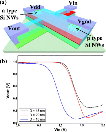
To implement 3d cmos inverter, only one half of the structure shown in figure s5b (supporting information) is required. A detailed circuit diagram of a cmos inverter is shown in figure 3. The pmos transistor is connected between the pow. N and p denote the (w/l) ratios of qn and qp, respectively, of the basic inverter. Cmos (complementary mos) technology uses both nmos and pmos transistors fabricated on the. As you can see from figure 1, a cmos circuit is composed of two mosfets. Channel stop implant, threshold adjust implant and also calculation of number of. (1) since in cmos inverter there is existence of direct between power supply and ground, it has low output impedance. Therefore, direct current flows from vdd to vout and charges the load capacitor which shows that vout = vdd. In this work, we focus on s3dc because it uses a static circuit style and fits well into the commercial cad tools based asic design flow. Manufacturing difficulties of vertically stacked source and drain electrodes of the cfets have been overcome by using junctionless transistors, thereby reducing the number of lithographic steps required. As you can see from figure 1, a cmos circuit is composed of two mosfets. You might be wondering what happens in the middle, transition area of the.


0 Response to "Cmos Inverter 3D / Cmos Wikipedia"
Post a Comment